
New Applications of Electron Holography Using Digital Technology
Highlight
While recent years have heightened interest in technologies for resolving environmental challenges that can help bring the global environment back within safe planetary boundaries, including devices with ultra-low power consumption and catalysts that can offer benefits in applications such as hydrogen production, the transformation of CO2 into a resource, and the decomposition of plastics, the design of high-performance materials and devices requires understanding of the electric and magnetic fields that underly the manifestation of these functions.
Hitachi has developed electron microscopy techniques for the atomic-scale observation of these phenomena in which electron holography plays a key role. In recent years, this has also included the use of digital technologies to perform observations that would not be possible using hardware on its own.
This article describes three such applications, namely measurement of the electric charge on catalyst nanoparticles, automatic nanoparticle measurement, and the observation of lattice plane magnetic fields.
1. Introduction
Achieving an environmentally neutral society calls for decarbonization technologies in the green energy sector and techniques for lower power consumption and thermal dissipation in the digital device sector. Moreover, developing these technologies will require the discovery of fundamentally new material properties together with their optimal combination and control. The basis of device function lies in the arrangement of atoms. Augmenting this structural information with the acquisition of high-resolution information about the electric and magnetic fields that are deeply intertwined with functionality can be extremely useful for analyzing problems and elucidating mechanisms in a wide range of technology development work.
Electron holography is a useful technique for high-resolution observation of the electromagnetic field distribution in localized regions. It works by measuring changes in the wavefront (phase) of electron waves. To achieve the ultimate resolution, Hitachi developed an atomic-resolution holography electron microscope in 2014 that features an aberration corrector and an acceleration voltage of 1.2 MV with support from the Funding Program for World-Leading Innovative R&D on Science and Technology (FIRST)1). More recently, combining the atomic-resolution holography electron microscope with digital technologies has enabled a number of extreme measurements that would not have been possible by enhancements to the hardware alone. This article describes further new advances in three such measurements, namely measurement of the electric charge on catalyst nanoparticles, automatic nanoparticle measurement, and the observation of lattice plane magnetic fields.
2 Enhancements and Applications for Atomic-resolution Holography Electron Microscopy Paired with Digital Technology
2.1 Use of Information Science in Measurement of Electric Charge on Catalyst Nanoparticles
Catalysts that promote a wide variety of chemical reactions are important substances, having a part to play in resolving global-scale problems such as cleaning up the environment and increasing food production. Electron holography is recognized as an important technique for uncovering the properties of these catalysts. It uses measurements of electron wave phase to determine the distribution of electric potential in and around a material. For the extremely small electric charges and potential distribution exhibited by catalyst nanoparticles, however, measurement required a major technical leap in the form of an order-of-magnitude improvement in phase measurement accuracy. To take on this challenge, Hitachi partnered with Kyushu University, Akashi College of the National Institute of Technology (KOSEN), and Osaka University in a joint research group, pursuing their own distinctive research strategy that combined the latest techniques of electron microscopy with methods from information science (techniques for extracting very weak signals).
Recognizing that the quality of the hologram image data was an important factor in the phase measurement accuracy of electron holography, the work paid particular attention to image quality and to the extraction of very weak signals. Achieving an order-of-magnitude improvement in the phase measurement accuracy of a hologram has been a long-standing challenge. When measurement time (quantity of incident electrons) is considered, for example, improving phase measurement accuracy by an order of magnitude would require it to be 100 times longer than conventional practice. Unfortunately, this would still not achieve the desired accuracy. The problem is that prolonged exposure of an electron wave changes or damages the specimen and so there is a limit to how much the measurement time can be extended. To overcome this problem, in addition to using the 1.2-MV atomic-resolution holography electron microscope that features world-leading performance for electron wave coherency (a characteristic with a close relationship to hologram image quality), the team also developed and adopted methods from information science, including the use of a wavelet hidden Markov model*1 to separate the very weak signal from the noise. This fusion of leading-edge measurement and information technology succeeded in achieving the order-of-magnitude improvement in the phase measurement accuracy of electron holography, something that would not have been possible using past approaches. This phase measurement accuracy makes possible new research into catalysts beyond what could be achieved by other measurement techniques, providing the ability to quantify the charge on individual nanoparticles with single-electron accuracy.
Figure 1—Charge State on Single Pt Nanoparticles on TiO2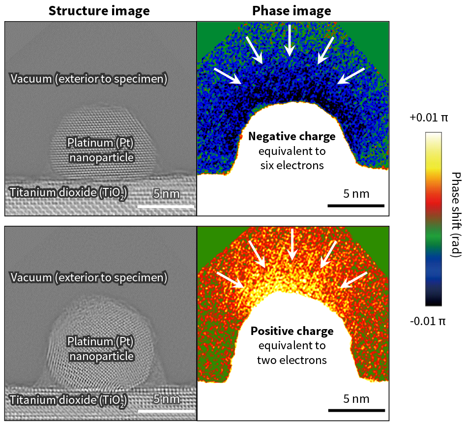 The upper and lower images show negatively and positively charged Pt nanoparticles, respectively. It is possible to determine the charge and polarity of Pt nanoparticles with high precision from the spatial distribution of catalyst electric potential.
The technique has been used to make precise studies of the distribution of electric potential in platinum-titanium dioxide (Pt/TiO2) catalysts that are widely used in applications such as cleaning up the environment2) (see Figure 1). By using phase measurement in the vicinity of a Pt nanoparticle to determine the spatial distribution of electric potential, it is possible to obtain the electric charge of a specific Pt nanoparticle of interest that is supported on a TiO2 substrate. The upper and lower images in Figure 1, for example, show nanoparticles with charges equivalent to six and two electrons, respectively. These studies were able to provide extremely useful knowledge for catalyst research and development, including for example that the Pt nanoparticles may be positively or negatively charged depending conditions at the boundary where they are attached to the TiO2 substrate, and that their electric charge is influenced by the amount of strain in the nanoparticle crystal. It is hoped that electron holography with ultra-high sensitivity will accelerate the development of catalysts that can help to resolve global environmental problems.
- *1
- A noise reduction method for image data. The wavelet transformation of image data has a tendency to carry those pixel characteristics that correspond to signal over to the corresponding transformed pixels. Accurate separation of signal from noise is achieved by using a number of Markov parameters (probability variables) to represent this tendency and then optimizing these parameters. The name “wavelet hidden Markov model” comes from how, in its representation of the parameters, the technique utilizes the concept of hidden states from probability theory and statistics.
2.2 Automatic Electron Holography Measurement of Nanoparticles
Data-driven research has become increasingly prominent in the field of electron microscopy over recent years, progressing in step with advances in information processing technology3). The extraction of common features from large amounts of data has enabled the visualization of nano-scale structures, electromagnetic characteristics, and other such features that could not be observed using conventional microscopy. Unfortunately, the acquisition of data has often been a bottleneck in such research. Development of the technique described above that uses electron holography for the quantitative measurement of electric charge on catalyst nanoparticles has revealed that nanoparticle electric charge varies widely2). Elucidating the charging mechanism requires the observation of many nanoparticles, creating a need for a technique that can acquire large numbers of hologram images with atomic resolution. One existing technique for doing so has been to scan the view field progressively step by step. Unfortunately, the use of conventional automated measurement techniques has resulted in a low percentage of available data, e.g. particles are not visible in the image or particles are shifted significantly from the image center. In response, a technique that can search for desired particles and efficiently acquire hologram images including the nanoparticles was developed by incorporating an image classifier that uses pattern matching and convolutional neural network (CNN) machine learning 4), 5).
Figure 2—TEM Image Used to Identify Particles for Automatic Hologram Measurement (a) and Phase Image Reconstructed from Automatically Acquired Hologram Image (b)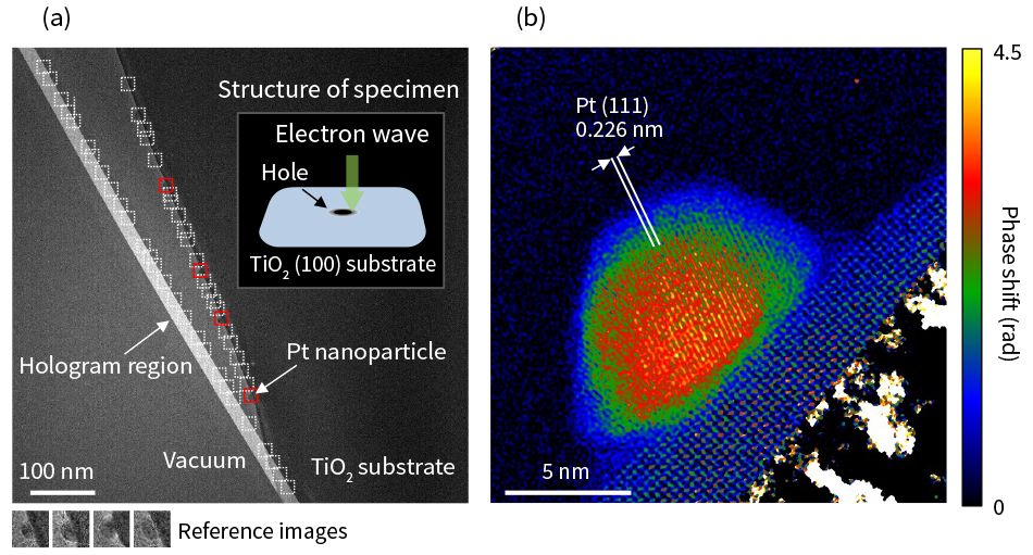 The microscope was used to observe a specimen prepared by forming a hole in the center of a TiO2 substrate and supporting Pt nanoparticles around the thinned edge of the hole. The dotted-line squares in image (a) indicate regions identified by pattern matching as having high similarity and the red squares indicate regions identified by the image classifier as containing a particle.
The technique acquires low-magnification images by means of a transmission electron microscope (TEM) and then uses pattern matching to identify the locations in these images that have a high degree of similarity with reference images used for comparison. Images showing the region around these locations are cut out and recorded along with location information. Next, the image classifier is used to determine which of these cut-out images contain nanoparticles, and high-magnification hologram images of only the corresponding locations are only acquired. Figure 2 shows an example of this automatic measurement. Figure 2 (a) is a TEM image used for particle detection. It shows the hologram regions where interference occurs between the electron waves and the Pt nanoparticles supported on the TiO2 substrate. When pattern matching was performed using the four reference images shown at the bottom-left, the results still included the detection of many locations that did not contain any of the Pt nanoparticles, such as the edges of the TiO2 substrate (indicated by the dotted-line squares). However, when the image classifier was used to decide whether or not Pt nanoparticles were present, it achieved an accuracy of more than 80% (indicated by the red squares). Figure 2 (b) shows a phase image reconstructed from the acquired hologram image. The data acquired by this study achieved the spatial resolution and positional accuracy of observation required for the electric charge analysis of all the nanoparticles and the data acquisition efficiency was improved around 100-fold compared to the scanning method used in the past. As the task of machine learning was simple for only sorting images into two different classes, the method has been able to achieve a high classification accuracy despite using only around 200 images as training data for the CNN. When applying the method to unknown specimens, the total time for the data collection and the training can be reduced. This means that it is possible to quickly respond to changes in the shape of specimens that are required during research and development..
2.3 Use of Digital Aberration Correction for Observation of Lattice Plane Magnetic Field
Figure 3—Schematic Diagram of Observation Method and Successful Observation of Lattice Plane Magnetic Field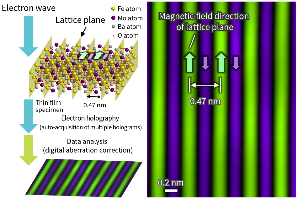 Fe: iron, Mo: molybdenum, Ba: barium, O: oxygenThe figure shows the distribution of magnetic fields in individual (111) lattice planes of a magnetic material (Ba2FeMoO6 crystal) in which the magnitude and orientation of the magnetic fields are different for each atomic plane.
Analysis of the magnetic structure of materials and the related characteristic of spin arrangement plays an important part not only in solid state physics, inorganic chemistry, and spintronics, but also in fields such as materials science and engineering. Unfortunately, direct observation of magnetic fields at the atomic level has been difficult to achieve in the past when performing magnetic field analysis on specimens such as those with variable thickness or where a number of different elements are involved in the magnetic field.
With support from JST-CREST (JPMJCR1664)*2, a joint research group involving Hitachi, Kyushu University, the Institute of Physical and Chemical Research (RIKEN), HREM Research Inc., the National Institute of Advanced Industrial Science and Technology (AIST), and the National Institute for Materials Science (NIMS) developed a technique that uses the atomic-resolution holography electron microscope to observe magnetic fields in specimens with non-uniform structure or composition that have proved difficult to observe in the past, such as multilayer magnetic films. Using the developed technique, they were the first in the world to successfully perform magnetic field observations for individual lattice planes of a material6) (see Figure 3).
The method combines an automatic electron holography technique that maintains atomic resolution with a digital aberration correction technique that automatically corrects the focus (aberration) after automatic acquisition. By integrating and averaging large amounts of data, automatic acquisition is able to obtain highly accurate measurements of weak magnetic field information at the atomic level. The difficulty is that maintaining optimal focus for all the many measurements collected during automatic acquisition is not easy. To address this, the research group developed a data analysis system that performs post-measurement digital aberration correction by analyzing the data after the experiment ends. Performing aberration correction after electron hologram measurements have been completed was the very reason why the Hungarian physicist Dénes Gábor developed holography in the first place. Aberration correction has been performed by both optical means and by digital processing. However, performing digital aberration correction automatically using large quantities of data requires a means of automatically analyzing aberrations in measurement data. The analysis system used here automated the process by applying an aberration correction technique7) to electron holography that works by analyzing object waves*3 acquired from regions of amorphous carbon to measure the residual aberration. By doing so it realized magnetic field observations at the interfaces between regions of different materials at the level of atomic planes6).
This high-resolution observation technique has applications not only in magnetic observations but also has wider applications in the measurement of various other specimen types, such as the high-resolution measurement of electric potential in catalysts and the visualization of atomic potential in devices.
- *2
- A research program run by the Japan Science and Technology Agency with the aim of fostering the creative and promising seeds of innovative new technologies based on new scientific knowledge.
- *3
- Electron waves carrying amplitude and phase information that have passed through a specimen.
3. Conclusions
By incorporating digital technology into the atomic-resolution holography electron microscope, Hitachi is pioneering new applications of electron holography that make use of digital methods. In addition to contributing to the progress of basic science through the elucidation of chemical reaction fields or magnetic phenomena taking place at the atomic level, it is anticipated that this technology can also play a role in developing high-performance magnets and high-function catalysts for the electrification applications that will facilitate decarbonization and the achievement of a carbon-neutral society, and assist with the development of energy-efficient devices that will reduce the energy use required across all aspects of our daily lives.
Acknowledgments
This work was funded through the Japan Society for the Promotion of Science (JSPS) by the Cabinet Office’s FIRST Program and received support from JST CREST (JPMJCR 1664). The research described in this article also received considerable assistance from everyone involved, including Professor Yasukazu Murakami and Associate Professor Ryotaro Aso of Kyushu University and Dr. Yoshinori Tokura, Dr. Daisuke Shindo, Dr. Xiuzhen Yu, and Dr. Ken Harada of RIKEN. The authors would like to take this opportunity to express their deep gratitude to all collaborators.
REFERENCES
- 1)
- T. Akashi et al., “Aberration corrected 1.2-MV cold field-emission transmission electron microscope with a sub-50-pm resolution,” Applied Physics Letters, 106, 074101 (Feb. 2015).
- 2)
- R. Aso et al., “Direct identification of the charge state in a single platinum nanoparticle on titanium oxide,” Science, 378, pp. 202-206 (Oct. 2022).
- 3)
- S. R. Spurgeon et al., “Towards data-driven next-generation transmission electron microscopy,” Nature Materials, 20, pp. 274-279 (Oct. 2021).
- 4)
- F. Ichihashi et al., “Improved efficiency in automated acquisition of ultra-high-resolution electron holograms using automated target detection,” Microscopy, 70, pp. 510-518 (Jun. 2021).
- 5)
- F. Ichihashi et al, “Automatic electron hologram acquisition of catalyst nanoparticles using particle detection with image processing and machine learning,” Applied Physics Letters, 120, 064103 (Feb. 2022).
- 6)
- T. Tanigaki et al., “Electron Holography Observation of Individual Ferrimagnetic Lattice Planes,” Nature, 631, pp. 521-525 (Jul. 2024).
- 7)
- Y. Taniguchi et al., ”Correction of spherical aberration in HREM image using defocus-modulation image processing,” Journal of Electron Microscopy, 41, pp. 21-29 (Feb. 1992).