
Smart Technology for More Efficient Semiconductor Development, Maintenance, and Production
Highlight
The ever-growing importance of semiconductor devices over recent years has been driving demand for improved manufacturing performance, especially for leading-edge devices. Moreover, semiconductor manufacturing facilities are becoming ever more automated, pushing ahead with DX and adopting smart manufacturing concepts.
Meanwhile, the semiconductor manufacturing industry is confronting the challenges that come with the adoption of smart practices across a range of areas, including processes, production equipment, and process integration. In response, Hitachi has been developing solutions that support digital twins for these different areas.
This article focuses on the optimization of process conditions development, making maintenance more efficient, and shortening development timelines for process integration, describing the research and development of smart techniques for resolving the challenges that these goals pose.
1. Introduction
Semiconductor devices have grown in importance over recent years in step with advances in the technology of artificial intelligence (AI). Amid calls for improvement in manufacturing performance, especially for leading-edge devices, semiconductor manufacturing facilities are pushing ahead with digital transformation (DX) and are adopting smart manufacturing concepts as they become ever more automated1). As semiconductor manufacturing involves many different processes, it is important that this DX be achieved across a wide range of areas.
In response, Hitachi has been developing solutions that support digital twins for manufacturing. This has involved developing and trialing solutions for: (1) Processes (an AI technique that searches for process conditions automatically), (2) Equipment (technology for smarter practices in maintenance), and (3) Process integration (a technique for in-line electrical properties measurement). In addition to contributing to semiconductor device manufacturing performance, these initiatives are also intended to enable more efficient semiconductor production by encouraging automation and DX at semiconductor manufacturing facilities to accelerate the establishment of smart factories.
2. Automatic Search AI for Process Conditions
The production process for semiconductor devices is becoming increasingly complex as they adopt three-dimensional architectures such as gate-all-around (GAA) in pursuit of performance. The etching process used to fabricate nano-scale structures is one area where development timelines for process conditions (recipes) are getting longer as these recipes come to have increasing numbers of steps and parameters. By using an AI to analyze the relationships between process conditions and the etching profile , which is imaged and quantified using an electron microscope, Hitachi’s newly developed AI technique can search for optimal process conditions automatically2), 3).
The inability to acquire sufficient data for training optimization models is one of the challenges facing this field. A feature of the new technique, however, is that it improves the accuracy of optimal conditions search by performing model training in an iterative manner, working through a cycle of (a) Data consolidation, (b) Machine learning, (c) Optimal conditions search, and (d) Experimental verification, as shown in Figure 1. Use of the technique helps to shorten the development timeline for etching process conditions.
Figure 1—Sequence of Steps for Optimizing Process Conditions and Etching Profile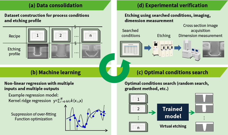 The accuracy of optimal conditions search is enhanced by working through a cycle of (a) Data consolidation, (b) Machine learning, (c) Optimal conditions search using a trained model, and (d) Experimental verification of the conditions identified.
Figure 2(a) shows the best etching profile obtained for the initial training data and after cycles one, three, and seven when optimization was performed for vertical fabrication of a pattern with a trench width of 750 nm. This technique succeeded in making the trench deeper and more vertical with less surface roughness after each cycle. Figure 2(b) demonstrates the viability of optimization of leading-edge nano-scale fabrication using the AI technique by showing the evaluation result of the optimized etching profile with a trench width and line width of 12.5 nm.
Figure 2—Example Results of Optimization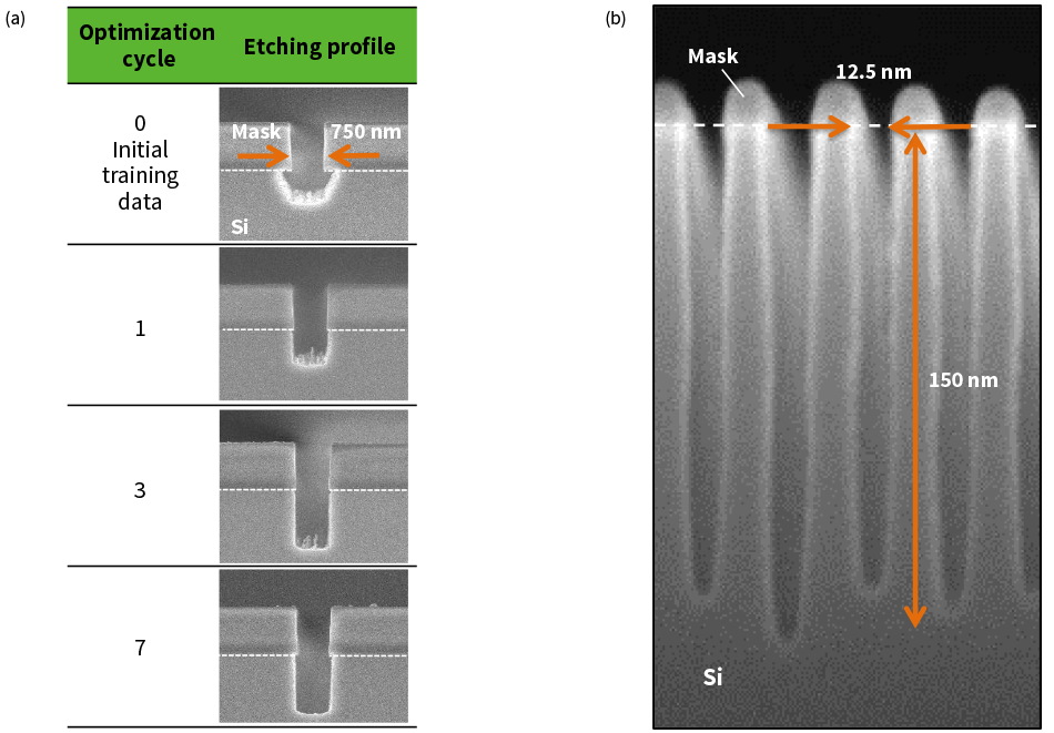 Image (a) shows the etching profile improvements after each optimization cycle when the target profile was a vertical trench with a width of 750 nm. Whereas the initial training data had 72 conditions, the number of conditions after condition search and experimental verification for optimization cycles one through seven were five, 14, five, seven, five, seven and eight conditions, respectively. The condition search is used to identify conditions that are expected to achieve a good profile. Image (b) shows the optimized result to obtain a vertical profile with a trench width and line width of 12.5 nm.
3. Smart Technology for Maintenance
Even as they become increasingly automated, there are still many tasks in a semiconductor manufacturing facility that require human resources. Equipment maintenance is one of these. As the success or failure of equipment maintenance is in large part due to the skill of the service engineer, there is growing demand for smart maintenance not only to improve the level of work, but also to overcome workforce shortages (with skilled workers especially in short supply).
In response, Hitachi has developed a three-dimensional (3D) technique that can acquire worker measurements, including field-of-view, head position, and hand movements, and analyze their actions and how they handle parts and materials (see Figure 3). The technique can use the measurement data to analyze the differences between experienced and inexperienced workers. Its capabilities include assessing highly skilled or difficult tasks and determining which actions are important to perform them successfully. One example is that the technique can calculate the angular velocity distribution of wiping actions and use this to analyze things like the direction of the wiping motion, where the worker’s attention is focused, how close they are to the equipment, and their hand movement speed4), 5), 6).
In addition to precise monitoring of work performance, this 3D measurement and analysis technique can also replicate it in a virtual environment. Hitachi intends to utilize this to offer solutions that help with things like remote work support, the acquisition and archiving of work logs, and worker upskilling. This involves developing a remote work support system in which a single skilled worker can support multiple workplaces (see Figure 4). The system will enable a remotely located skilled worker to see what is happening in the workplace and instruct on-site workers on the correct manual actions to perform, using technologies such as virtual reality to give them the ability to freely shift their viewpoint while viewing workplaces in real time. This means they can provide assistance and show by example how to perform tasks in much the same way as when on-the-job-training (OJT) is done on-site. By doing so, on-site workers can resolve any problems that might arise with equipment maintenance without the skilled worker having to visit the site. Hitachi intends to continue developing smart maintenance techniques like this, and to roll the technology out for maintenance work in a wide range of other sectors in tandem with its ongoing support for the semiconductor manufacturing industry.
Figure 3—3D Work Measurement Technique for Smart Maintenance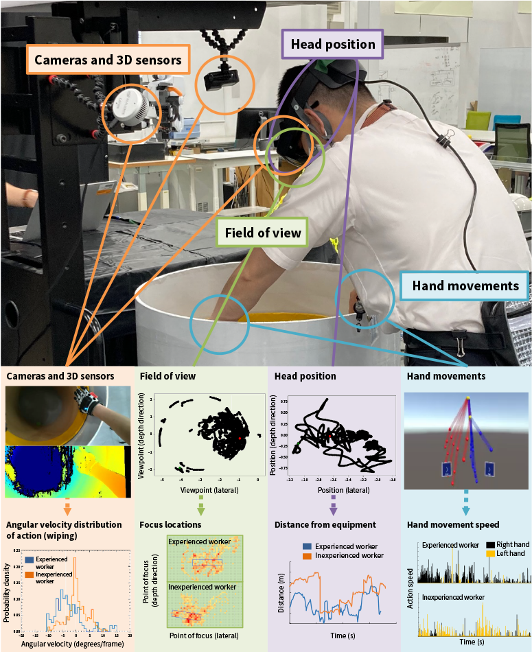 The technique uses cameras and other 3D sensors to measure things like field of view, head position, and hand movements. It uses this measurement data to analyze the differences between experienced and inexperienced workers and assess things like difficult or highly skilled tasks and which actions are important to perform them successfully. One example is that the technique can calculate the angular velocity distribution of wiping actions and use this to analyze things like the direction of the wiping motion, where the worker’s attention is focused, how close they are to the equipment, and their hand movement speed.
Figure 4—Overview of New Remote Work Support System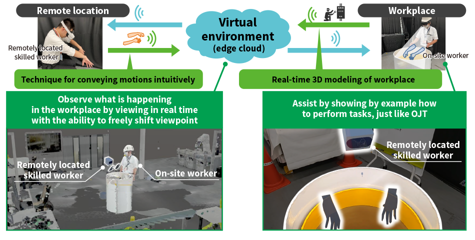 OJT: on-the-job-trainingHitachi is addressing workforce shortages by developing a remote work support system that a small number of skilled workers can use to support a large number of sites. The system uses technologies such as virtual reality to let remotely located skilled workers see what is happening in the workplace, giving them the ability to freely shift their viewpoint while viewing the workplace in real time. This allows them to provide assistance and show by example how to perform tasks in much the same way as on-site OJT.
4. In-line Electrical Properties Measurement
Improving productivity is an urgent issue for semiconductor manufacturing as the number of process steps involved continues to accelerate. Inspections such as dimensional measurement and checking for particles that are performed between each process step play an important part in ensuring production line reliability. Unfortunately, the shift to 3D device structures and the growing diversity of materials means that an increasing number of defects cannot be detected by checking geometric abnormalities such as dimensions or particles. Such defects in materials or in the circuits on the wafer cannot be detected until probe testing is performed in the latter stages of production.
This is driving demand for in-line electrical properties measurement that can check for electrical defects or abnormalities in material properties on the production line, thereby providing timely feedback to the production process.
To meet this need, Hitachi is developing a laser-assisted scanning electron microscope (LA-SEM) that shines a laser on the specimen and performs inspections of the electrical and material properties of circuits and other patterns based on measurements derived from how they respond to the incident light and electron beam [see Figure 5(a)]. The technique has successfully measured capacitance and other electrical properties and it can also acquire contrast information that is indicative of material damage. Figure 5(b) shows a sample that was fabricated to test static capacitance measurement and the measurement results obtained. The ability to perform highly accurate capacitance measurement was verified by fabricating tiny plug-shaped specimens with a range of different capacitance values and then demonstrating a correlation between the results of using the LA-SEM to acquire indicative values that correspond to capacitance and the design capacitance values calculated from the plug dimensions7). Figure 5(c) shows the imaging of damage done to an insulating film. Test samples were prepared by deliberately damaging selected parts of SiO2 film specimens by exposing them to plasma. By using the LA-SEM to perform surface potential measurements on these samples, it was demonstrated that differences indicative of damage that cannot be detected by a conventional SEM can instead be quantified in terms of differences in surface potential8).
By doing so, this has provided proof-in-principle that the development of this technique makes it possible to quantitatively measure capacitance and insulation film damage.
Figure 5—LA-SEM Diagram and Uses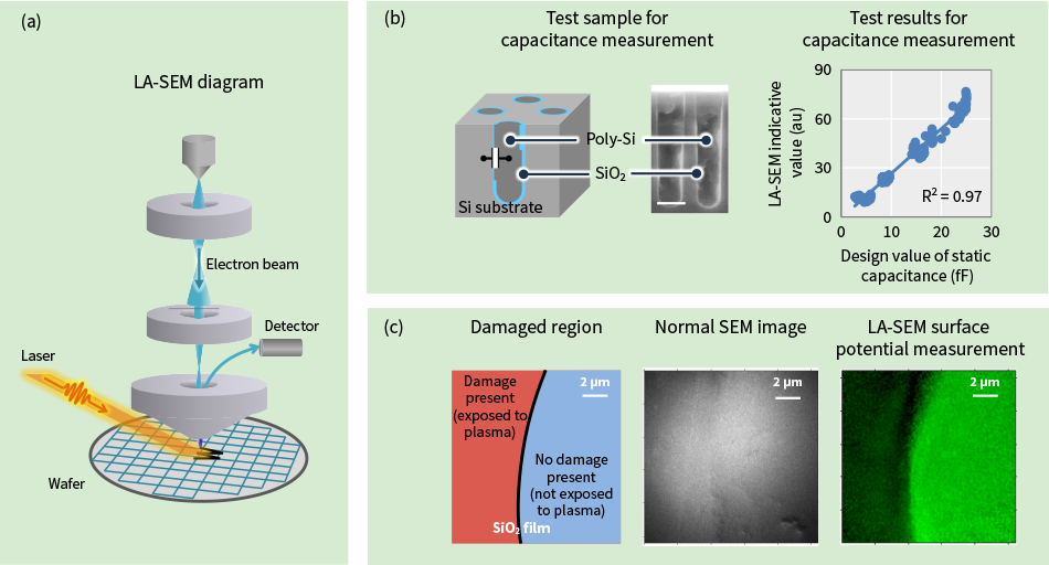 LA-SEM: laser-assisted scanning electron microscopeImage (a) shows a diagram of an LA-SEM, (b) shows test results for capacitance measurement, and (c) shows test results for measurement of film damage.
5. Conclusions
By continuing its work on commercializing these technologies and packaging them in solutions for the semiconductor manufacturing industry, Hitachi intends to contribute to smarter semiconductor manufacturing by facilitating DX in the respective areas of development, maintenance, and production. In parallel, Hitachi also intends to further enhance its group presence by seeking to roll the technologies out to other forms of manufacturing that are grappling with similar challenges.
REFERENCES
- 1)
- Semiconductor Equipment and Materials International (SEMI), “SEMI:Smart Manufacturing Initiative Works to Help Chip Industry Achieve Industry 4.0 Ambitions,” (Sep. 2022).
- 2)
- T. Ohmori et al., “Prediction and Optimization of Etching Profile Using Machine Learning,” Proceedings of International Symposium on Dry Process (DPS), p. 9 (2017).
- 3)
- T. Dobashi et al., “Effect of initial-learning dataset on etching profile optimization using machine learning in plasma etching,” Japanese Journal of Applied Physics, 62, SI1016 (Jun. 2023).
- 4)
- T. Numata et al.,”Experimental 3D maintenance work measurement and analysis for maintenance improvement and enhancement of productivity of semiconductor manufacturing equipment,” AVS 69th International Symposium & Exhibition, MS-ThP-3, p. 192 (2023).
- 5)
- T. Numata et al.: Metaverse-based remote support system with smooth combination of free viewpoint observation and hand gesture instruction,” Journal of the Society for Information Display, 32, 8 (Jul. 2024).
- 6)
- Hitachi, Ltd., “Development of technology that links virtual and real worlds for efficient remote supervision by skilled personnel of on-site workers engaged in equipment inspection and repair work: Supervisors have a free view of the worksite and can show models to on-site workers using the hand movements of an avatar,” (Mar. 2023) in Japanese.
- 7)
- S. Minami et al., “Laser assisted SEM for visualizing electrical property using voltage contrast dynamics,” Proceedings, the international society for optics and photonics (SPIE), 12496, 1249630 (2023).
- 8)
- Y. Shirasaki et al., “Evaluation of thin-film material properties using laser-assisted SEM,” Proceedings, SPIE, 12955, 129551K (2024).