
New FineSAT 7 Scanning Acoustic Tomograph for Non-destructive Testing of Advanced Semiconductor Devices
Highlight
Security of supply for the semiconductors that underpin digitalization is becoming an issue for societies around the world. Scanning acoustic tomographs are ultrasound imaging systems used in non-destructive testing to view the device interior of semiconductors or other electronic components. Hitachi is deploying this technique for non-destructive testing to contribute to overcoming these societal challenges.
Recent advances in semiconductor miniaturization, multi-layer chips, and high-density mounting have placed greater demands on the performance of inspection systems. This article describes the technologies developed for the FineSAT 7, which was released in 2022 as the top-end model in the FineSAT series. The development goal for the FineSAT 7 was to expand functionality for the non-destructive testing of advanced devices.
1. Introduction
Semiconductors are more than just foundational products that underpin the digitalization of society, they are also important strategic goods in terms of economic security. With long-term demand expected to be driven by the growth of digitalization, the secure supply of semiconductors with guaranteed reliability is recognized as an issue for societies around the world.
Scanning acoustic tomographs (SATs) are non-destructive testing systems that can image the device interior of semiconductors or other electronic components. Hitachi supplies a range of SAT products to suit diverse user needs, notably the FineSAT series, which delivers highly detailed images.
In the semiconductor industry, Hitachi SATs are mainly used at the packaging stage for fault analysis and screening where their non-destructive testing capabilities help to ensure semiconductor reliability and security of supply. Recent advances in semiconductor miniaturization, multi-layer chips, and high-density mounting have progressively increased the technical difficulty of the defect detection work that SATs perform. As manufacturing workplaces use fewer people, there has also been strong demand for improvements in work efficiency and the automation of the inspection process. Hitachi has a track record of delivering user support functions to help overcome these customer challenges(1), (2), (3).
This article describes the technologies developed for the FineSAT 7, which was released in 2022 as the top-end model in the FineSAT series. Along with further enhancing techniques for achieving high image quality, an area where Hitachi was already strong, the development of the FineSAT 7 also included the addition of useful functions for improving productivity and work efficiency.
2. Overview of FineSAT
Figure 1—FineSAT 7 Scanning Acoustic Tomograph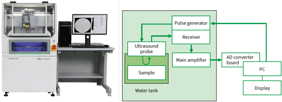 AD: analogue-to-digital The photograph on the left shows the FineSAT 7 housing and PC, and the block diagram on the right shows the signal flow.
Figure 1 shows how imaging works in a FineSAT system. The sample being inspected is placed in a tank filled with water that serves as a medium for the ultrasound and then the ultrasound probe is positioned above it. The probe converts the electrical pulses from the pulse generator into ultrasonic waves, shapes these into a beam, and directs it at the sample. The probe also converts the received ultrasound (both reflected and transmitted) back to an electrical signal.
The analogue-to-digital (AD) converter board is equipped with an AD converter and a field-programmable gate array (FPGA) that transform the analog electrical signal into digital form and perform digital signal processing functions such as filtering. After this conversion to digital waveform data in the AD converter board, the electrical signal from the probe is passed to a PC where the image is generated by software. The probe in the SAT is linked to a scanner that scans in a two-dimensional pattern, building up a two-dimensional image by progressively acquiring and processing the waveform data.
3. New AD Converter Board with Enhanced Technology for High Image Quality
Figure 2—Comparison of Images from FineSAT 7 and Previous Model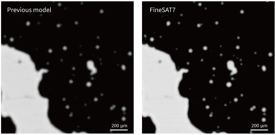 The images show internal voids in bonded wafers. While both images show a large bright void on the left, a number of smaller voids are also present on the right. FineSAT 7 can show smaller voids than the previous model.
Improving the signal resolution of the waveform data can help to acquire the extremely weak signal generated by microscopic defects. This signal resolution refers to the smallest differences in the electrical signal input to the AD converter board that the system is able to recognize. For example, if an AD converter board with 8-bit resolution is used to convert an ultrasound electrical signal in the −250 mV to +250 mV range into waveform data it will be able to distinguish differences of 500 / 28 ≃ 1.95 mV.
As higher signal resolution increases the cost of digital signal processing by the FPGA, logical operation design technologies are needed that can execute the required processing in the available time while keeping the calculation scale the same as before. To achieve this, Hitachi developed a logical operation technology that involves temporarily storing the data awaiting processing in first-in first-out (FIFO) memory buffers and using time-division processing synchronized with probe scanning to reduce the large calculation scale. Use of this design technology improved signal resolution by a factor of 16 compared to previous Hitachi models while keeping the digital circuit for FPGA to a practical size.
Having a higher signal resolution enables image data to be acquired with a high dynamic range (HDR), making it possible to identify detailed features across the entire image even in samples where the differences in brightness are large. In the past, insufficient dynamic range in the imaging of such samples has resulted in white-out saturation in bright pattern regions or microscopic defects being obscured in dark regions. With the use of appropriate data compression techniques, however, the detailed information contained in images with a high dynamic range can be preserved, improving the visibility of microscopic defects without white-out of the bright patterns, even when displayed on a screen with low dynamic range (see Figure 2).
4. Analysis Software to Support Assessment of Semiconductor Reliability
The use of analysis software is essential to improving work efficiency and automating the inspection process. Hitachi draws on its extensive experience in the semiconductor industry to offer software for functions such as image sharpening(3), (4) and automatic defect identification(5). This section highlights functions that it is anticipated will be useful for advanced semiconductors in particular.
4.1 Support Function for Gate Setting (Waveform Simulator)
Figure 3—Waveform Simulator Screen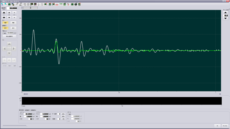 The screen shows the graphical user interface (GUI) for the waveform simulator. The white line shows the predicted waveform data for a multi-layer sample and the colored line highlights the echoes from the chip in the first layer.
Gate setting refers to the user specifying a time window (gate) by means of the graphical user interface (GUI)(3). The SAT obtains its image of the interior of the sample using the intensities of those echoes that are within the gate range. This means that the user must specify a range that will include echoes from the boundary surface they want to image.
The waveform data from multi-layer chips that feature in advanced semiconductor devices contains numerous multipath reflection echoes as well as the echoes from individual layers. Considerable experience is generally needed to specify the gate setting for waveform data that contains such complex patterns.
However, it is possible to predict the time range in which echoes will occur by calculating the ultrasound delay times from the speed of sound and layer thicknesses. Moreover, the waveform data collected by the SAT can be treated as a superposition of the ultrasound waves that have followed each of the different possible paths. Utilizing this insight, Hitachi developed a computer simulator that can track the ultrasound propagation pathways and predict the acquired waveform data. In addition to ultrasound delay, the simulator can also replicate physical phenomena such as the changes in amplitude, phase inversions, and multipath reflection that result from reflection and transmission.
The GUI displays the predicted waveform data in response to user entry of information about the sample’s layer structure that includes the materials and thicknesses. The user selects the layer they are interested in to highlight the echoes from that layer (see Figure 3). The user can then make use of this information when choosing the gate time range.
4.2 Noise Cancelling (Waveform Averaging)
Figure 4—Use of Waveform Averaging for Noise Cancelling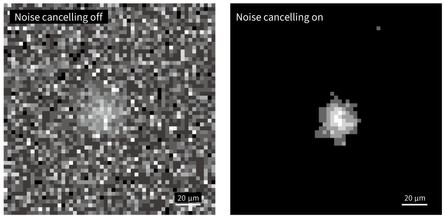 The images show a 5-µm artificial defect inside bonded wafers. While the defect is visible in the center of both images, the noise level is reduced and it becomes much more easily visible when waveform averaging is enabled.
The waveform data passed from the AD converter board to the PC contains random electrical noise that can interfere with the detection of microscopic defects. A feature of semiconductor inspection applications is that they require the detection of defects that are smaller than the diameter of the ultrasound beam. Unfortunately, such small defects produce a very weak signal that is similar in intensity to the noise level.
One method used to reduce random noise is averaging, whereby the waveform data contained in the signal of interest is integrated multiple times and averaged. However, this method is slower than normal operation because it requires the scanner to remain still long enough to acquire the data needed for integration.
To overcome this problem, Hitachi has devised a novel signal processing algorithm that can perform averaging without halting scanning (patent No. 7201864). This works by including data from adjacent measurement points in the waveform data being integrated and averaged. As the waveform data includes values that are divergent or displaced in the time axis, the data is screened using pattern analysis and displacement compensation is also performed. This preprocessing can reduce random noise while retaining the signals that actually derive from the sample, such as defects.
Noise can degrade visibility when a SAT is used to image defects of a few micrometers in size. As use of this newly developed technique can reduce the level of ambient noise without loss of defect signals, it delivers superior visibility and contrast (see Figure 4).
5. Large Water Tank for Transmission Inspection of Entire 300-mm Wafer
Demand for transmission inspection has risen in recent years for use on multi-layer chips. As transmission inspection involves the synchronized scanning of separate transmitter and receiver probes, it is performed using an arm-shaped apparatus. This restricts the scanner movement range compared to reflection inspection because of the risk of collision between the arm and other components. When using the previous model to acquire images of an entire 300-mm wafer, this constraint meant that probe scanning needed to be performed twice, with the wafer being repositioned manually between scans.
When the FineSAT 7 was developed, the layout of equipment in the vicinity of the sample was revised to enlarge the water tank while keeping the same footprint as the previous system. The additional scanner movement range this provides means that an entire 300-mm wafer can be inspected in a single scan (see left of Figure 5). When using a standard tray as specified by the Joint Electron Device Engineering Council (JEDEC), it is also possible to specify the address area for the underside of the sample. This makes the system easier to operate, allowing for the insertion of an apparatus for eliminating bubbles on the sample underside (see right of Figure 5).
Figure 5—Large Water Tank on FineSAT 7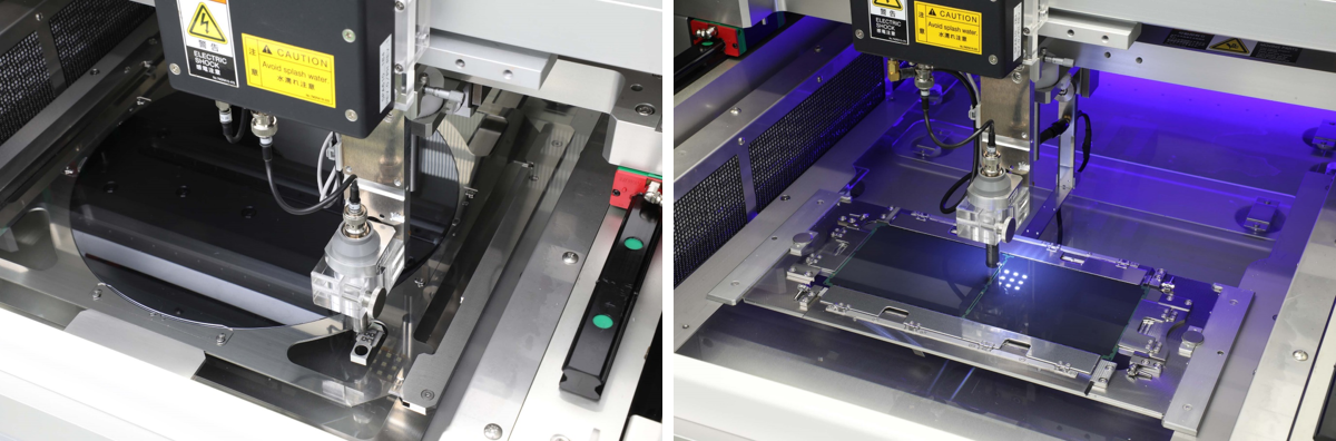 The photographs show a 300-mm wafer (left) and the FineSAT 7 water tank with a JEDEC-standard tray inserted (right).
6. Conclusions
The FineSAT 7 was developed with additional functions needed for the non-destructive testing of advanced devices. It features a new AD converter board, further enhancements to Hitachi’s already advanced techniques for high image quality, and improvements to user work efficiency and productivity made using both software and hardware. In recognition of these new technologies, FineSAT 7 won the 65th Top 10 New Products Award sponsored by Nikkan Kogyo Shimbun in 2022(6). Hitachi intends to contribute to the resolution of societal challenges by continuing to develop functions that benefit users.
REFERENCES
- 1)
- H. Yamamoto et al., “Scanning Acoustic Tomograph to Accelerate Development of Surface Mount Process” in Japanese, Hitachi Hyoron, 91, pp. 468–471 (May 2009).
- 2)
- K. Kitami et al., “Ultrasonic Imaging of Microscopic Defects to Help Improve Reliability of Semiconductors and Electronic Devices,” Hitachi Review, 65 pp. 272–276 (Aug. 2016).
- 3)
- S. Ohno et al., “Nondestructive Ultrasonic Testing Systems for Safe and Reliable Electronics: Hitachi FineSAT Series and ES Series of Scanning Acoustic Tomographs,” Hitachi Review, 68, pp. 121–126 (Jan. 2019).
- 4)
- K. Sakai et al., “Image improvement using image processing for scanning acoustic tomograph images,” 2015 IEEE 22nd International Symposium on the Physical and Failure Analysis of Integrated Circuits (IPFA), pp. 163–166 (2015).
- 5)
- K. Sakai et al., “Defect detection method using statistical image processing of scanning acoustic tomography,” 2016 IEEE 23rd International Symposium on the Physical and Failure Analysis of Integrated Circuits (IPFA), pp. 293–296 (2016).
- 6)
- Hitachi News Release, “Scanning Acoustic Tomograph "FineSAT 7" for Non-destructive Testing of Electronic Device Wins 65th Top 10 New Products Award” in Japanese (Jan. 2023).